02 - Electrical — IceDrone V3.4
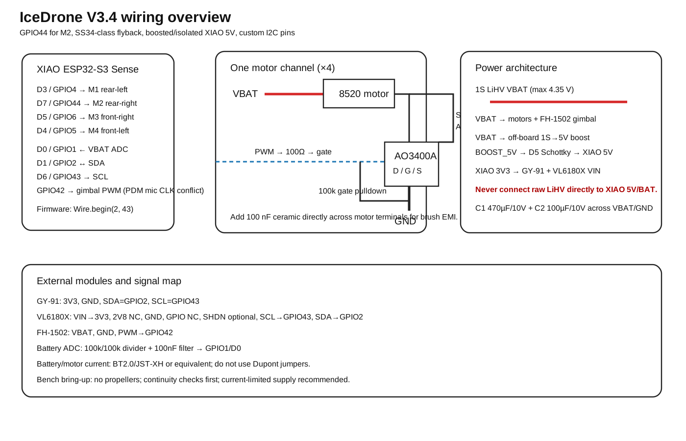
Authoritative machine-readable files:
hardware/motor_stage_netlist.csvhardware/pinmap.csvhardware/perfboard_v34_netlist.csvhardware/perfboard_v34_pin_matrix.csv
Revision note: V3.4 supersedes the earlier V1/V3.2/V3.3 electrical notes. In particular, M2 uses GPIO44/D7 instead of GPIO3, D1-D4 are SS34-class flyback diodes, the XIAO is powered from a regulated 5 V boost path, and the photographed VL6180X module has a verified seven-pin order.
Power architecture
IceDrone V3.4 uses a raw 1S LiHV VBAT rail for the brushed motors and the FH-1502 gimbal. A fully charged 1S LiHV cell can reach 4.35 V.
The XIAO ESP32-S3 Sense is not connected directly to raw VBAT in this revision. Use:
VBAT → off-board 1S→5V boost → D5 Schottky → XIAO 5V
The common ground is shared. The XIAO's regulated 3V3 output then powers the GY-91 and the VL6180X breakout.
Required suppression and filtering
- C1: 470 µF / 10 V low-ESR across VBAT/GND
- C2: 100 µF / 10 V low-ESR across VBAT/GND
- C3: 100 nF ceramic from VBAT_ADC to GND, in parallel with R10
- D1-D4: SS34-class ≥3 A Schottky flyback diodes
- one additional 100 nF ceramic directly across each motor's terminals
- short, wide VBAT/GND/motor-current wiring
- twisted motor wire pairs where practical
- keep ADC and I2C wiring away from motor drain/PWM wiring
Motor driver channel
Each motor is low-side switched by an AO3400A:
flowchart LR
    VBAT --> MOTOR["8520 motor"] --> DRAIN["Motor− / MOSFET drain"]
    DRAIN --> Q["AO3400A"] --> GND
    DRAIN --> DIODE["SS34 ≥3 A<br/>anode = drain<br/>cathode/band = VBAT"] --> VBAT
    GPIO -->|"100 Ω"| GATE["MOSFET gate"]
    GATE -->|"100 kΩ"| GND
The gate pulldown is mandatory because it holds the MOSFET off while the ESP32 GPIO is high impedance during boot.
AO3400A pinout
For the SOT-23 AO3400A package:
- pin 1 = Gate
- pin 2 = Source
- pin 3 = Drain
On perfboard use a SOT-23 adapter or very short dead-bug leads. Do not infer the electrical node from the physical drawing alone; follow the netlist.
GPIO map
| Function | XIAO pin / GPIO | Notes |
|---|---|---|
| M1 rear-left | D3 / GPIO4 | PWM |
| M2 rear-right | D7 / GPIO44 | PWM; changed from GPIO3 in V3.4 |
| M3 front-right | D5 / GPIO6 | PWM |
| M4 front-left | D4 / GPIO5 | PWM |
| Battery ADC | D0 / GPIO1 | 100k/100k divider + 100 nF filter |
| I2C SDA | D1 / GPIO2 | GY-91 + VL6180X |
| I2C SCL | D6 / GPIO43 | GY-91 + VL6180X |
| Gimbal PWM | GPIO42 test pad | conflicts with Sense PDM microphone clock |
GPIO3 is intentionally left unused in V3.4. The Sense camera GPIO set and microSD GPIO7/8/9/21 are preserved.
I2C requirement
Because GPIO5 and GPIO6 are motor PWM outputs, do not rely on the XIAO default I2C pins.
Firmware must explicitly initialize:
Wire.begin(2, 43);
Battery measurement
R9 and R10 form a 100k/100k divider:
VBAT → R9 → VBAT_ADC → R10 → GND
C3 = 100 nF is placed in parallel with R10 to suppress motor brush noise.
Nominally:
V_ADC = VBAT / 2
At 4.35 V battery voltage the ADC node is about 2.175 V.
In firmware start with:
VBAT = V_ADC * 2.0
and calibrate against a multimeter.
VL6180X — photographed module
With the actual module front side visible, text upright and header at the bottom, the physical pin order is:
VIN | 2V8 | GND | GPIO | SHDN | SCL | SDA
V3.4 uses:
- VIN → XIAO 3V3
- GND → common GND
- SCL → GPIO43 / D6
- SDA → GPIO2 / D1
- SHDN → optional / normally NC
- 2V8 → NC
- GPIO → NC
Do not connect the module's 2V8 output to the XIAO 3V3 rail.
Perfboard coordinate convention
The 70×30 mm perfboard uses this fixed convention:
| View | left → right | top → bottom |
|---|---|---|
| component side | A B C D E F G H I J | 1…24 |
| solder side | J I H G F E D C B A | 1…24 |
A1-A24= VBATJ1-J24= GNDE12= unused
The detailed construction guide and rear-view solder map are in 10 - Perfboard V3.4 soldering.
Current-separation rule
Dupont/breadboard jumper wires are only for low-current module and signal connections.
Do not route battery or 8520 motor current through Dupont jumpers. Use BT2.0/JST-XH or equivalent appropriately rated wiring/connectors for battery and motor current.
Before connecting the XIAO
- continuity-test VBAT-to-GND; no hard short may be present;
- verify every MOSFET source is at GND;
- verify each drain is only on its own motor−/flyback node;
- verify D1-D4 cathode bands point toward VBAT;
- verify D5 cathode points toward XIAO 5V;
- verify C1/C2 polarity;
- verify raw VBAT has no direct path to XIAO 5V;
- verify boost output before connecting the XIAO;
- first power-up with propellers removed and preferably with a current-limited bench supply.
← 01 - BOM | Docs index | Next: 03 - Mechanical →